In the rapidly evolving world of electronics, the demand for more efficient, smaller, and more powerful devices has never been higher. From smartphones and computers to automotive lighting and industrial applications, cutting-edge technologies depend heavily on the materials that form their foundation. Among these, High-Purity Alumina (HPA) has emerged as a critical enabler, particularly in the fields of LED technology and semiconductor manufacturing. Its exceptional purity, thermal stability, and chemical resistance make it indispensable for next-generation electronics.
At Jiangsu Shengtian New Materials Co., Ltd., we have witnessed firsthand how HPA transforms both performance and reliability in advanced applications. In this article, we explore why HPA is considered the backbone of LED and semiconductor technology, discuss its properties and manufacturing methods, and highlight its critical role in driving innovation across multiple industries.
Understanding High-Purity Alumina
What is High-Purity Alumina?
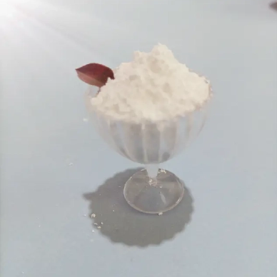
High-Purity Alumina, or Al₂O₃, is a refined form of aluminum oxide with purity levels typically exceeding 99.99%. Unlike standard alumina used in ceramics or abrasives, HPA is produced under stringent conditions to remove impurities such as sodium, iron, and silicon that could interfere with electronic performance. These impurities, even in trace amounts, can affect the optical, thermal, and electrical properties essential for LED and semiconductor applications.
HPA is available in powder, single-crystal, and polycrystalline forms, each tailored for specific industrial applications. The material’s high melting point, thermal conductivity, and dielectric strength make it particularly suitable for devices that require extreme precision and stability under high-temperature operating conditions.
Key Properties Driving Electronics Innovation
Several key properties make HPA essential in next-generation electronics:
Exceptional Purity: Trace impurities can drastically affect optical and electrical performance. HPA’s ultra-pure composition ensures minimal interference.
High Thermal Conductivity: Effective heat dissipation is critical for LEDs and semiconductor devices to prevent degradation.
Chemical Stability: HPA remains stable in harsh chemical environments, ensuring longevity in semiconductor manufacturing processes.
Dielectric Strength: Its excellent insulation properties enable high-performance electronics with minimal energy loss.
These properties collectively enhance device reliability, efficiency, and lifespan, which is why HPA is preferred for demanding applications in the LED and semiconductor sectors.
HPA in LED Technology
Enhancing Light Output and Efficiency
In LED applications, HPA serves primarily as a substrate and phosphor carrier. For phosphor-converted LEDs (PC-LEDs), HPA’s transparency and thermal conductivity enable efficient light conversion and heat dissipation, enhancing brightness and overall efficiency. By reducing thermal resistance, HPA helps maintain color stability and prolongs LED operational life.
High-quality HPA substrates also allow the fabrication of thin, uniform phosphor layers, which are essential for next-generation high-lumen LEDs used in automotive headlights, display backlighting, and industrial lighting solutions.
Thermal Management in LEDs
LEDs generate heat during operation, and excessive heat can degrade the semiconductor material, reducing both efficiency and lifespan. HPA’s high thermal conductivity provides a robust solution for heat management, conducting heat away from sensitive areas while maintaining optical clarity. This makes HPA crucial for high-power LEDs where thermal stress is a limiting factor.
HPA in Semiconductor Manufacturing
Supporting Wafer Production
In semiconductor manufacturing, HPA plays a role in producing high-purity sapphire wafers, which are used for LEDs and advanced semiconductors. Sapphire substrates offer mechanical robustness, high thermal conductivity, and electrical insulation, all of which are essential for the reliability of microelectronic devices.
HPA’s exceptional purity ensures that these wafers are free from defects that could compromise device performance. Even minor contamination could cause dislocations or irregularities in crystal growth, leading to decreased yields and higher manufacturing costs.
Enabling Next-Gen Chips
As semiconductor nodes shrink and device density increases, materials like HPA are critical to meeting tight tolerances and ultra-clean manufacturing requirements. HPA contributes to:
High-quality insulation layers
Stable dielectric performance
Uniform thermal characteristics for lithography and epitaxial processes
This makes it a backbone material in producing advanced semiconductors for smartphones, servers, and automotive electronics.
Manufacturing and Processing of HPA
Refining Aluminum to HPA
The production of HPA involves precise chemical and thermal processes to achieve ultra-high purity levels. Common methods include:
Bayer Process-derived alumina: Purification through precipitation and calcination
Aluminum chloride or aluminum sulfate conversion: Produces high-purity powders suitable for electronics
Hydrothermal growth: Produces single-crystal sapphire for semiconductor wafers
Each method is carefully controlled to minimize trace impurities, ensuring that the final HPA product meets the stringent standards required for LED and semiconductor applications.
Powder vs. Crystal Forms
Powdered HPA is commonly used as a raw material for phosphor coatings and polycrystalline substrates.
Single-crystal HPA is grown into sapphire wafers for high-performance LEDs and semiconductors, offering superior thermal and mechanical properties.
Choosing the appropriate form depends on the application, whether for light-emitting devices, insulating layers, or high-temperature substrates.
Innovations Driving HPA Applications
High-Power LEDs
Recent innovations in HPA-enabled substrates have allowed the development of high-power LEDs for industrial, automotive, and architectural lighting. These LEDs maintain performance even under extreme temperatures and prolonged operation, largely due to HPA’s thermal management capabilities.
Micro-LEDs and Miniaturization
As display technology moves toward micro-LEDs, HPA is crucial in providing transparent, high-purity substrates that support precise phosphor deposition and thermal stability. This facilitates higher pixel density, improved brightness, and longer lifespan for next-generation displays.
Advanced Semiconductors
In semiconductor fabrication, HPA is enabling smaller nodes and higher integration density, supporting high-speed computing, AI processors, and 5G communication chips. Its purity and structural stability are fundamental to producing chips that meet modern performance and reliability requirements.
Benefits of HPA in Electronics
Reliability and Longevity
HPA enhances the durability and operational lifespan of LEDs and semiconductors by providing thermal stability and preventing degradation under high-power operation.
Efficiency and Performance
By improving heat dissipation and supporting high-quality substrates, HPA ensures devices operate at higher efficiency with consistent performance, even under demanding conditions.
Cost-Effectiveness in the Long Term
While HPA may represent a premium material, its impact on reducing device failures, improving yield, and extending operational life makes it cost-effective for manufacturers and end-users alike.
Sustainability Considerations
Advanced HPA production techniques minimize impurities and reduce waste, supporting more sustainable electronic manufacturing. Additionally, its role in improving energy efficiency in LEDs contributes to broader environmental benefits.
Future Trends and Opportunities
Expansion in Automotive Electronics
Electric vehicles and advanced driver-assistance systems (ADAS) rely on high-performance LEDs and semiconductors. HPA substrates support the development of durable, high-brightness LEDs for headlights, displays, and sensors, driving demand in the automotive sector.
IoT and Smart Devices
The Internet of Things (IoT) requires compact, reliable semiconductors with high thermal and electrical performance. HPA enables miniaturized components that meet the stringent reliability requirements of smart devices.
Emerging Manufacturing Techniques
Techniques like additive manufacturing and advanced crystal growth methods are expanding the possibilities for HPA-based components, allowing more customized shapes, higher purity, and improved thermal properties for next-gen electronics.
Conclusion
High-Purity Alumina (HPA) is indisputably the backbone of next-generation LED and semiconductor technology. Its exceptional purity, thermal conductivity, chemical stability, and dielectric strength make it a critical material for enhancing device performance, reliability, and efficiency. From high-power LEDs and micro-LED displays to advanced semiconductor wafers, HPA supports innovations that are shaping the future of electronics.
From an industry perspective, Jiangsu Shengtian New Materials Co., Ltd. is at the forefront of supplying high-quality HPA for LED and semiconductor applications. Engineers, manufacturers, and technology developers seeking reliable, high-purity materials are encouraged to contact Jiangsu Shengtian New Materials Co., Ltd. to explore tailored solutions that meet the demanding requirements of modern electronic technologies.
FAQ
Q: What is High-Purity Alumina (HPA)?
A: HPA is aluminum oxide with purity levels exceeding 99.99%, used for substrates, insulation, and thermal management in electronics.
Q: Why is HPA critical for LED technology?
A: HPA provides thermal conductivity, transparency, and stability for phosphor layers and substrates, enhancing brightness and efficiency.
Q: How does HPA support semiconductor manufacturing?
A: HPA enables defect-free sapphire wafers and insulating layers, supporting precise lithography and high-performance chip production.
Q: Can HPA improve the lifespan of electronic devices?
A: Yes. Its chemical stability and thermal management reduce degradation, improving device reliability and longevity.


